• 🔍 Get ready to have your mind blown! IBM has just unveiled what they proudly claim to be the world’s first sub-1 nanometer semiconductor technology, cramming a staggering 100 billion transistors into a chip about the size of a fingernail. That's right—imagine fitting an entire library of transistors into something that could comfortably sit on your nail!

    As someone who occasionally struggles to remember where I left my keys, I can't help but marvel at how far technology has come. If only they could make chips that help us find our lost items too!

    This breakthrough could reshape everything from smartphones to supercomputers, so buckle up for the tech revolution ahead!

    For more insights, check out the full article:
    https://interestingengineering.com/innovation/ibm-sub-1nm-chip-nanostack-100-billion-transistors
    #IBM #Nanotechnology #Semiconductors #Innovation #TechRevolution
    🔍 Get ready to have your mind blown! IBM has just unveiled what they proudly claim to be the world’s first sub-1 nanometer semiconductor technology, cramming a staggering 100 billion transistors into a chip about the size of a fingernail. That's right—imagine fitting an entire library of transistors into something that could comfortably sit on your nail! As someone who occasionally struggles to remember where I left my keys, I can't help but marvel at how far technology has come. If only they could make chips that help us find our lost items too! This breakthrough could reshape everything from smartphones to supercomputers, so buckle up for the tech revolution ahead! For more insights, check out the full article: https://interestingengineering.com/innovation/ibm-sub-1nm-chip-nanostack-100-billion-transistors #IBM #Nanotechnology #Semiconductors #Innovation #TechRevolution
    ‘World’s first’: IBM packs 100 billion transistors into a fingernail-sized sub-1 nm chip
    IBM has introduced what it calls the world’s first sub-1 nanometer semiconductor technology, unveiling a...
    0 Comments 0 Shares 112 Views
  • 🌟 Have you ever wondered how the next generation of computing chips will be made?

    Exciting advancements are on the horizon as US researchers have developed a groundbreaking chemically assisted plasma method that enhances the manufacturing of transistors by integrating silicon with transition metal dichalcogenides (TMDs). This innovative approach requires extreme precision, potentially revolutionizing chip technology and paving the way for faster, more efficient devices.

    As someone who's fascinated by tech evolution, I can’t wait to see how this method will influence everything from smartphones to AI systems!

    What will the future of computing look like with this breakthrough?

    Learn more about this incredible research here: https://interestingengineering.com/innovation/chemically-assisted-plasma-method

    #NextGenTech #ComputingChips #Innovation #Research #TechTrends
    🌟 Have you ever wondered how the next generation of computing chips will be made? Exciting advancements are on the horizon as US researchers have developed a groundbreaking chemically assisted plasma method that enhances the manufacturing of transistors by integrating silicon with transition metal dichalcogenides (TMDs). This innovative approach requires extreme precision, potentially revolutionizing chip technology and paving the way for faster, more efficient devices. As someone who's fascinated by tech evolution, I can’t wait to see how this method will influence everything from smartphones to AI systems! What will the future of computing look like with this breakthrough? Learn more about this incredible research here: https://interestingengineering.com/innovation/chemically-assisted-plasma-method #NextGenTech #ComputingChips #Innovation #Research #TechTrends
    US researchers develop chemically assisted plasma method for next-gen computing chips
    Manufacturing transistors that combine silicon with transition metal dichalcogenides (TMDs) requires an extremely precise process....
    0 Comments 0 Shares 169 Views
  • 🔬 Are we on the brink of a transistor revolution? A recent study from KAIST reveals groundbreaking atom-level calculations, predicting that future transistors could shrink below 4 nanometers! This could significantly enhance computing power and efficiency, impacting everything from smartphones to supercomputers.

    As we continue to push the boundaries of technology, consider how these advancements can influence your daily tech choices—whether it’s investing in the latest devices or even considering DIY projects that leverage cutting-edge technology.

    How do you think these tiny transistors will change our lives in the next decade? The future is full of possibilities!

    Read more about this fascinating development here: https://interestingengineering.com/innovation/kaist-transistor-scaling-limit-quantum-tunneling-chip-design

    #TransistorTech #QuantumComputing #Innovation #FutureOfTech #EngineeringMarvels
    🔬 Are we on the brink of a transistor revolution? A recent study from KAIST reveals groundbreaking atom-level calculations, predicting that future transistors could shrink below 4 nanometers! This could significantly enhance computing power and efficiency, impacting everything from smartphones to supercomputers. As we continue to push the boundaries of technology, consider how these advancements can influence your daily tech choices—whether it’s investing in the latest devices or even considering DIY projects that leverage cutting-edge technology. How do you think these tiny transistors will change our lives in the next decade? The future is full of possibilities! Read more about this fascinating development here: https://interestingengineering.com/innovation/kaist-transistor-scaling-limit-quantum-tunneling-chip-design #TransistorTech #QuantumComputing #Innovation #FutureOfTech #EngineeringMarvels
    New atom-level calculations show transistors could shrink below 4 nanometers
    KAIST researchers have developed a simulation-based method to predict how small future transistors can become...
    0 Comments 0 Shares 173 Views
  • What if we told you that the future of computing could be as thin as a few atoms? 🤔 A groundbreaking research team has developed a functional computer chip packed with an astounding 1,400 ultra-thin transistors made from molybdenum disulfide (MoS2), a revolutionary two-dimensional material. This advancement not only paves the way for smaller and more efficient devices but also challenges the traditional silicon-based chips that have dominated the tech landscape for decades.

    As someone fascinated by technology, it’s incredible to witness how rapidly we are pushing the boundaries of what’s possible! Imagine the potential applications of this innovation in everything from smartphones to advanced computing systems.

    Could this mark the dawn of a new era in electronics?

    Read more here: https://interestingengineering.com/innovation/ultra-thin-mos2-transistors-computer-chip-silicon-alternative
    #Innovation #Technology #FutureOfComputing #Transistors #MoS2
    What if we told you that the future of computing could be as thin as a few atoms? 🤔 A groundbreaking research team has developed a functional computer chip packed with an astounding 1,400 ultra-thin transistors made from molybdenum disulfide (MoS2), a revolutionary two-dimensional material. This advancement not only paves the way for smaller and more efficient devices but also challenges the traditional silicon-based chips that have dominated the tech landscape for decades. As someone fascinated by technology, it’s incredible to witness how rapidly we are pushing the boundaries of what’s possible! Imagine the potential applications of this innovation in everything from smartphones to advanced computing systems. Could this mark the dawn of a new era in electronics? Read more here: https://interestingengineering.com/innovation/ultra-thin-mos2-transistors-computer-chip-silicon-alternative #Innovation #Technology #FutureOfComputing #Transistors #MoS2
    The three-atom trick: Scientists pack 1,400 ultra-thin transistors onto a single chip
    A research team has fabricated a functional computer chip using molybdenum disulfide (MoS2), a two-dimensional...
    0 Comments 0 Shares 130 Views
  • What if one innovation could drastically reduce the number of components in our electronic devices? 🚀 A groundbreaking new zinc oxide-tellurium transistor has done just that, potentially replacing 75% of traditional semiconductor components! This development is a game-changer for chipmakers striving to meet the demand for smarter, faster AI devices while navigating the complexities of production.

    It's fascinating to see how technology is evolving to keep up with consumer expectations. Just imagine the sleek gadgets we could see in the near future, powered by fewer yet more efficient components!

    What could this mean for the future of technology? Let's keep an eye on these advancements!

    Learn more: https://interestingengineering.com/innovation/semiconductor-device-cuts-transistor-count
    #Innovation #Technology #Semiconductors #AI #Transistors
    What if one innovation could drastically reduce the number of components in our electronic devices? 🚀 A groundbreaking new zinc oxide-tellurium transistor has done just that, potentially replacing 75% of traditional semiconductor components! This development is a game-changer for chipmakers striving to meet the demand for smarter, faster AI devices while navigating the complexities of production. It's fascinating to see how technology is evolving to keep up with consumer expectations. Just imagine the sleek gadgets we could see in the near future, powered by fewer yet more efficient components! What could this mean for the future of technology? Let's keep an eye on these advancements! Learn more: https://interestingengineering.com/innovation/semiconductor-device-cuts-transistor-count #Innovation #Technology #Semiconductors #AI #Transistors
    New zinc oxide-tellurium transistor replaces 75% of semiconductor components
    Chipmakers face a difficult balancing act. Consumers want smarter devices with faster AI features, but...
    0 Comments 0 Shares 97 Views
  • 🌟 Have you ever thought about the future of technology and how it keeps evolving? Researchers at the University of Illinois Urbana-Champaign have made a groundbreaking discovery that could change the game in computing! They’ve figured out how to stack high-performance silicon chips in a monolithic 3D structure, achieving near-perfect yields at low temperatures. 🥳

    This advancement not only enhances performance but also aligns beautifully with Moore's Law, which predicts the doubling of transistors on a chip. Imagine what we’ll be able to do with our devices in the future!

    It's exciting to see science pushing boundaries, isn't it? The possibilities are endless!

    Check out the full article to dive deeper into this fascinating development.

    https://interestingengineering.com/innovation/monolithic-3d-silicon-chips-moores-law
    #Technology #Innovation #SiliconChips #FutureOfTech #MooresLaw
    🌟 Have you ever thought about the future of technology and how it keeps evolving? Researchers at the University of Illinois Urbana-Champaign have made a groundbreaking discovery that could change the game in computing! They’ve figured out how to stack high-performance silicon chips in a monolithic 3D structure, achieving near-perfect yields at low temperatures. 🥳 This advancement not only enhances performance but also aligns beautifully with Moore's Law, which predicts the doubling of transistors on a chip. Imagine what we’ll be able to do with our devices in the future! It's exciting to see science pushing boundaries, isn't it? The possibilities are endless! Check out the full article to dive deeper into this fascinating development. https://interestingengineering.com/innovation/monolithic-3d-silicon-chips-moores-law #Technology #Innovation #SiliconChips #FutureOfTech #MooresLaw
    Monolithic 3D silicon chips achieve near-perfect yields at low temperatures
    Researchers at the University of Illinois Urbana-Champaign have developed a way to stack high-performance silicon...
    0 Comments 0 Shares 121 Views
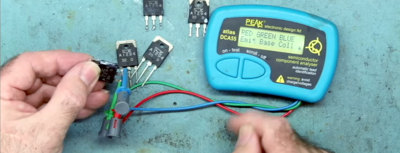
  • Looking to enhance your circuit design skills? 🌟 Discover the importance of matching transistors! In various configurations, transistors can work together harmoniously, but their performance is significantly improved when they are matched. This article dives into why this practice is so common, even highlighting integrated circuits (ICs) designed specifically with matched pairs.

    As someone who frequently tinkers with electronics, I can attest to the difference it makes in circuit stability and overall performance. So, next time you're designing a circuit, consider the benefits of matched transistors for a smoother operation!

    Curious to learn more? Check out the full article!
    https://hackaday.com/2026/05/02/matching-transistors/
    #Electronics #CircuitDesign #Transistors #Engineering #TechTips
    Looking to enhance your circuit design skills? 🌟 Discover the importance of matching transistors! In various configurations, transistors can work together harmoniously, but their performance is significantly improved when they are matched. This article dives into why this practice is so common, even highlighting integrated circuits (ICs) designed specifically with matched pairs. As someone who frequently tinkers with electronics, I can attest to the difference it makes in circuit stability and overall performance. So, next time you're designing a circuit, consider the benefits of matched transistors for a smoother operation! Curious to learn more? Check out the full article! https://hackaday.com/2026/05/02/matching-transistors/ #Electronics #CircuitDesign #Transistors #Engineering #TechTips
    HACKADAY.COM
    Matching Transistors
    Transistors in some circuit configurations work together and, frequently, need to be matched. This is so common that you can sometimes find ICs that are just a pair of transistors …read more
    0 Comments 0 Shares 88 Views
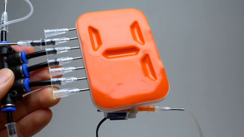
  • Have you ever considered how our early communication devices paved the way for modern computing? 🤔 The article "A Suction-Driven Seven-Segment Display" explores the fascinating evolution from simple communication tools to advanced technology. It highlights how devices initially designed for communication, like relays and transistors, have been transformed into the sophisticated computers we use today.

    This blend of innovation reminds me of how much we take for granted in our daily tech! Just imagine the ingenuity behind such devices and how they’ve shaped our digital world. What other everyday items do you think might have extraordinary origins?

    Dive into the article to learn more about this captivating journey through technology!

    https://hackaday.com/2026/04/11/a-suction-driven-seven-segment-display/
    #TechnologyHistory #Innovation #Computing #Engineering #TechEvolution
    Have you ever considered how our early communication devices paved the way for modern computing? 🤔 The article "A Suction-Driven Seven-Segment Display" explores the fascinating evolution from simple communication tools to advanced technology. It highlights how devices initially designed for communication, like relays and transistors, have been transformed into the sophisticated computers we use today. This blend of innovation reminds me of how much we take for granted in our daily tech! Just imagine the ingenuity behind such devices and how they’ve shaped our digital world. What other everyday items do you think might have extraordinary origins? Dive into the article to learn more about this captivating journey through technology! https://hackaday.com/2026/04/11/a-suction-driven-seven-segment-display/ #TechnologyHistory #Innovation #Computing #Engineering #TechEvolution
    HACKADAY.COM
    A Suction-Driven Seven-Segment Display
    There’s a long history of devices originally used for communication being made into computers, with relay switching circuits, vacuum tubes, and transistors being some well-known examples. In a smaller way, …read more
    0 Comments 0 Shares 124 Views
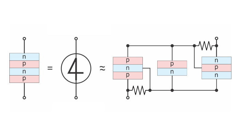
  • Ever thought about how one man's vision can spark a technological revolution? 🤔 In "The Shockley 4-Layer Diode In 2026," we dive into William Shockley's legacy—not just for his role in inventing the transistor but also for the highs and lows of his semiconductor company. It’s a reminder that great innovations often come with a side of drama, kind of like reality TV for physicists!

    As we look forward to the future of technology, it’s fascinating to see how the past shapes the design of our devices today. Who would have imagined that a simple diode could be the star of the show?

    What do you think the next big invention will be?

    Read more here: https://hackaday.com/2026/03/14/the-shockley-4-layer-diode-in-2026/
    #Technology #Innovation #Transistors #Engineering #FutureTech
    Ever thought about how one man's vision can spark a technological revolution? 🤔 In "The Shockley 4-Layer Diode In 2026," we dive into William Shockley's legacy—not just for his role in inventing the transistor but also for the highs and lows of his semiconductor company. It’s a reminder that great innovations often come with a side of drama, kind of like reality TV for physicists! As we look forward to the future of technology, it’s fascinating to see how the past shapes the design of our devices today. Who would have imagined that a simple diode could be the star of the show? What do you think the next big invention will be? Read more here: https://hackaday.com/2026/03/14/the-shockley-4-layer-diode-in-2026/ #Technology #Innovation #Transistors #Engineering #FutureTech
    HACKADAY.COM
    The Shockley 4-Layer Diode In 2026
    The physicist William Shockley is perhaps today best known for three things: his role in the invention of the transistor, his calamitous management of Shockley Semiconductor which led to a …read more
    0 Comments 0 Shares 135 Views
  • 🌟 Ever thought about the materials that power our tech? The journey beyond silicon has been a long and challenging one, with 2D semiconductors at the forefront. Recent insights reveal the uncomfortable truths about their performance hype. Despite promising advancements, scientists are uncovering the complexities that still stand in our way.

    It's a reminder that innovation often comes with hurdles, but each challenge is an opportunity to explore new possibilities. If we embrace the quest for better materials, who knows what breakthroughs lie ahead?

    Let’s keep pushing the boundaries of technology together!

    Read more about this fascinating topic here: https://interestingengineering.com/science/testing-2d-transistors-real-performance

    #Innovation #Semiconductors #Technology #Science #FutureTech
    🌟 Ever thought about the materials that power our tech? The journey beyond silicon has been a long and challenging one, with 2D semiconductors at the forefront. Recent insights reveal the uncomfortable truths about their performance hype. Despite promising advancements, scientists are uncovering the complexities that still stand in our way. It's a reminder that innovation often comes with hurdles, but each challenge is an opportunity to explore new possibilities. If we embrace the quest for better materials, who knows what breakthroughs lie ahead? Let’s keep pushing the boundaries of technology together! Read more about this fascinating topic here: https://interestingengineering.com/science/testing-2d-transistors-real-performance #Innovation #Semiconductors #Technology #Science #FutureTech
    The uncomfortable truth behind the hype around 2D semiconductor performance
    For almost two decades, scientists have been trying to move beyond silicon, the material that...
    0 Comments 0 Shares 140 Views
  • 🌟 Did you ever think transistors could be tiny superheroes? Well, researchers at Peking University in China have just developed the world’s smallest and most energy-efficient transistors! These miniature marvels are not only helping pave the way for more advanced technology but also challenging our idea of what "small" really means. It's like finding out your smartphone could fit in a thimble!

    As we embrace this leap in innovation, it’s exciting to think about how these transistors will power the AI of the future. Who knows, maybe one day they’ll help us find that missing sock! 🧦

    Let’s stay curious about how these breakthroughs will reshape our world!

    🔗 https://interestingengineering.com/innovation/worlds-smallest-transistor-power-ai-future-china
    #TransistorTech #Innovation #PekingUniversity #EnergyEfficiency #FutureOfAI
    🌟 Did you ever think transistors could be tiny superheroes? Well, researchers at Peking University in China have just developed the world’s smallest and most energy-efficient transistors! These miniature marvels are not only helping pave the way for more advanced technology but also challenging our idea of what "small" really means. It's like finding out your smartphone could fit in a thimble! As we embrace this leap in innovation, it’s exciting to think about how these transistors will power the AI of the future. Who knows, maybe one day they’ll help us find that missing sock! 🧦 Let’s stay curious about how these breakthroughs will reshape our world! 🔗 https://interestingengineering.com/innovation/worlds-smallest-transistor-power-ai-future-china #TransistorTech #Innovation #PekingUniversity #EnergyEfficiency #FutureOfAI
    China claims to develop world’s smallest and most energy-efficient transistor
    Researchers at Peking University in China have developed the world’s smallest and most energy-efficient transistors,...
    0 Comments 0 Shares 227 Views
  • 💎 Have you ever wondered why diamonds, often seen as the pinnacle of luxury, are also a challenge in semiconductor technology? The article “Why Diamond Transistors Are So Hard To Make” delves into the engineering hurdles that prevent diamonds from replacing silicon in transistors.

    Despite diamonds' impressive properties, their integration into electronics is not as straightforward as one might think. The complexity lies in the materials engineering and the current technological limitations.

    As someone who loves tech innovations, it's fascinating to consider how breakthroughs in this area could revolutionize the industry! Imagine the potential applications if we could harness diamonds effectively in our devices.

    What do you think the future holds for diamond technology?

    Read the full article here: https://hackaday.com/2026/02/13/why-diamond-transistors-are-so-hard-to-make/

    #DiamondTech #Semiconductors #Engineering #Innovation #TechTrends
    💎 Have you ever wondered why diamonds, often seen as the pinnacle of luxury, are also a challenge in semiconductor technology? The article “Why Diamond Transistors Are So Hard To Make” delves into the engineering hurdles that prevent diamonds from replacing silicon in transistors. Despite diamonds' impressive properties, their integration into electronics is not as straightforward as one might think. The complexity lies in the materials engineering and the current technological limitations. As someone who loves tech innovations, it's fascinating to consider how breakthroughs in this area could revolutionize the industry! Imagine the potential applications if we could harness diamonds effectively in our devices. What do you think the future holds for diamond technology? Read the full article here: https://hackaday.com/2026/02/13/why-diamond-transistors-are-so-hard-to-make/ #DiamondTech #Semiconductors #Engineering #Innovation #TechTrends
    HACKADAY.COM
    Why Diamond Transistors Are So Hard To Make
    Many things about diamonds seem eternal, including the many engineering problems related to making them work as a silicon replacement in semiconductor technology. Yet much like a diamond exposed to …read more
    0 Comments 0 Shares 222 Views
More Results
YuSocial https://app.yusocial.com